Designing the VCA
I struggled a bit with learning how to use the LM13700 as a VCA. I found the following resources helpful:
- LM13700 OTA Spec Sheet (TI)
- Aaron Lanterman VCA / OTA lecture (Youtube)
- “Vintage VCA” with LM13700 (Electric Druid)
Unlike a standard op-amp, the LM13700 is an operational transconductance amplifier (OTA); like an op-amp, it takes voltage as input, but unlike an op-amp it (a) amplifies based on a control current (termed ) rather than feedback voltage, (b) outputs a current (not a voltage). So, in order to use it as a VCA you have to (a) convert a control voltage into a control current, and (b) convert the output current into an output voltage.
Additionally, (c) optionally adding a diode bias current in order to reduce noise and (d) buffering the output which, unlike a standard op-amp, is high impedance.
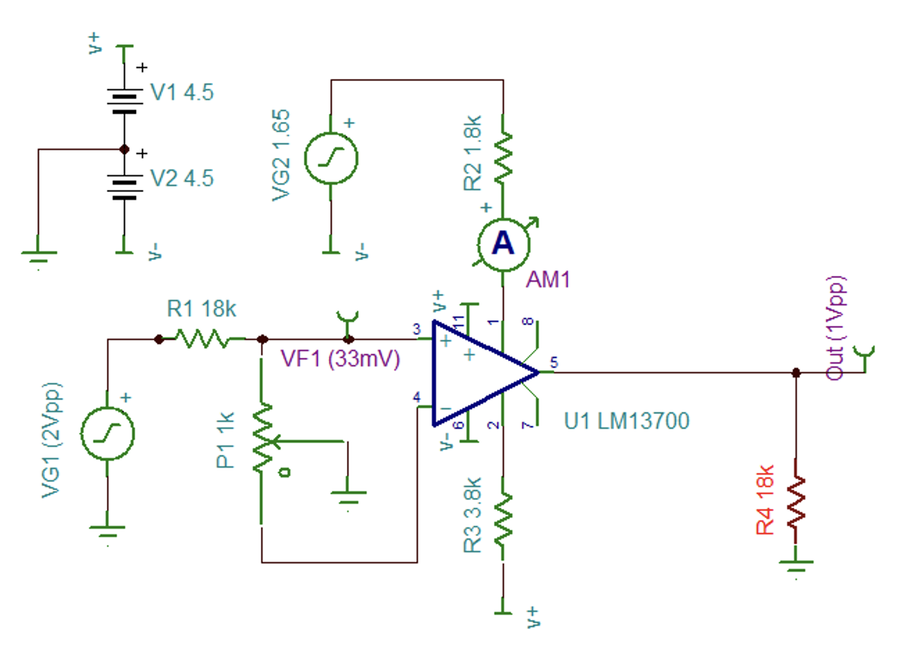
The circuit above is structurally the same as the example VCA circuit in the LM13700 spec sheet, but I’ve altered the values for the resistors to suit a 2Vpp input and +/- 4.5V power supply.
Note: For output buffering, I plan to use the same TL07X op amp I use elsewhere (not shown in the circuit above).
Ensuring Low THD
The LM13700 needs a low differential input voltage in order to limit “total harmonic distortion” (THD).
For the example circuit, the spec sheet suggests < 60mVpp (and using internal diodes) to target 0.1% THD.
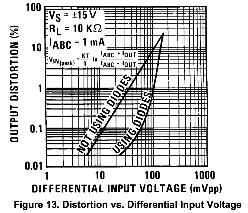
But, the chart will be different for a +/- 4.5v supply and 18K output current-to-voltage resistor. But perhaps not wildly different, so I will target 30mVpp in my circuit.
Using and input frequency of 1khz and an of 1mA, the fourier analysis in TINA TI suggests that the THD is 0.02%. Is this correct? I have no idea. I will make a THD measurement in the actual circuit once I build it.
Calculate R1 and P1 to attenuate the input voltage
Given that the input voltage to the circuit will be about 2Vpp (from pre-amp output), we attentuate the signal using a voltage divider to the target 30mVpp. This is an attenuation of about 1/67x.
NOTE: I’m using 18k / 500 divider and would expect that to yield only 1/37x attenuation. But, I get the full 1/67x in TINA TI. Hmm... perhaps due to internals of LM13700 (like diodes and/or impedance). Maybe I will learn more when I breadboard the circuit.
Calculate R2 to convert the control voltage to control current
I will be using the output of the microcontroller’s DAC which has a max of 3.3V. The bias input pin is two diode drops above the negative supply, which in our case gives a peak voltage of 3.3V - 1.4V = 1.9V. We want to set to 1ma at peak, giving us a desired R2 of 1.9K. Rounding to nearest common resistor value: 1.8K.
Calculate R4 to convert output current to voltage
The LM13700 provides a current dependent on the input voltage and control current. This current needs to be converted to voltage. We can use a resistor in parallel to do this. If we want 1Vpp, then following ohm’s law, .
can be calculated using the formula where is the “transconductance gain” a value that is dependent on temperature. Specifically, where is the “thermal voltage” which is approximately at 77 °F (room temperature). It’s common to use 25 or 26mV for .
NOTE: By adjusting in the simulated circuit, R4 needs to be 17.4K for an output of 1Vpp, not 1.74K (!!). I need to investigate why my calculations are off by a factor of 10 here. Maybe I’ll learn more when I breadboard the circuit.
Calculate R3 to apply current to the internal diodes
It is required that the diode bias current be greater than twice the input current. The input current has a DC level of 0; the diode bias is 1 diode drop above zero or 0.7V; tying the bias to V+ gives us a voltage drop of 4.5V - 0.7V = 3.9V across R3. targetting the recommended 1mA, we get R3 = 3.9V / 1mA = 3.9kΩ. Rounding to the nearest common, I get 3.8KΩ.
Simulating the circuit
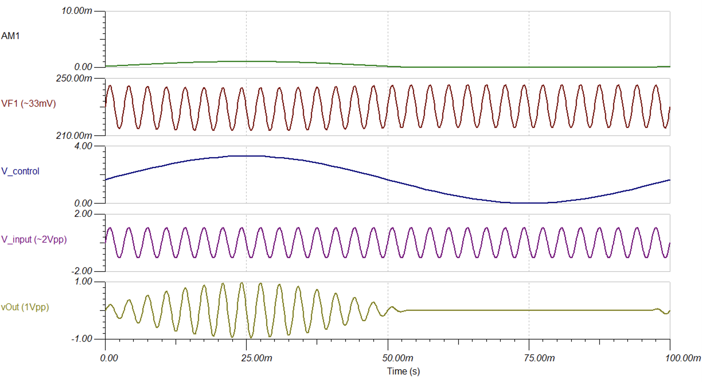
TINA TI schematic
- TINA schematic - This file is hosted on dropbox. Click the “download” button to download the file.
- ← Previous
Guitar pedal / ESP32 ADC trigger test - Next →
Regarding common grounds